- 您现在的位置:买卖IC网 > Sheet目录362800 > EVAL-AD421EB (Analog Devices, Inc.) Loop-Powered 4 mA to 20 mA DAC
AD421
–
8
–
REV. C
WORD "N"
0
1
1
0 0
1 1
0
0
0
0
0
0
0
0
0
0
CLOCK
DATA
(
(
B
B
B
B
B
B
B
B
B
B
B
B
B
B
B
B
LATCH
B
X X X X X X X
X
X
X
X
X
X
X
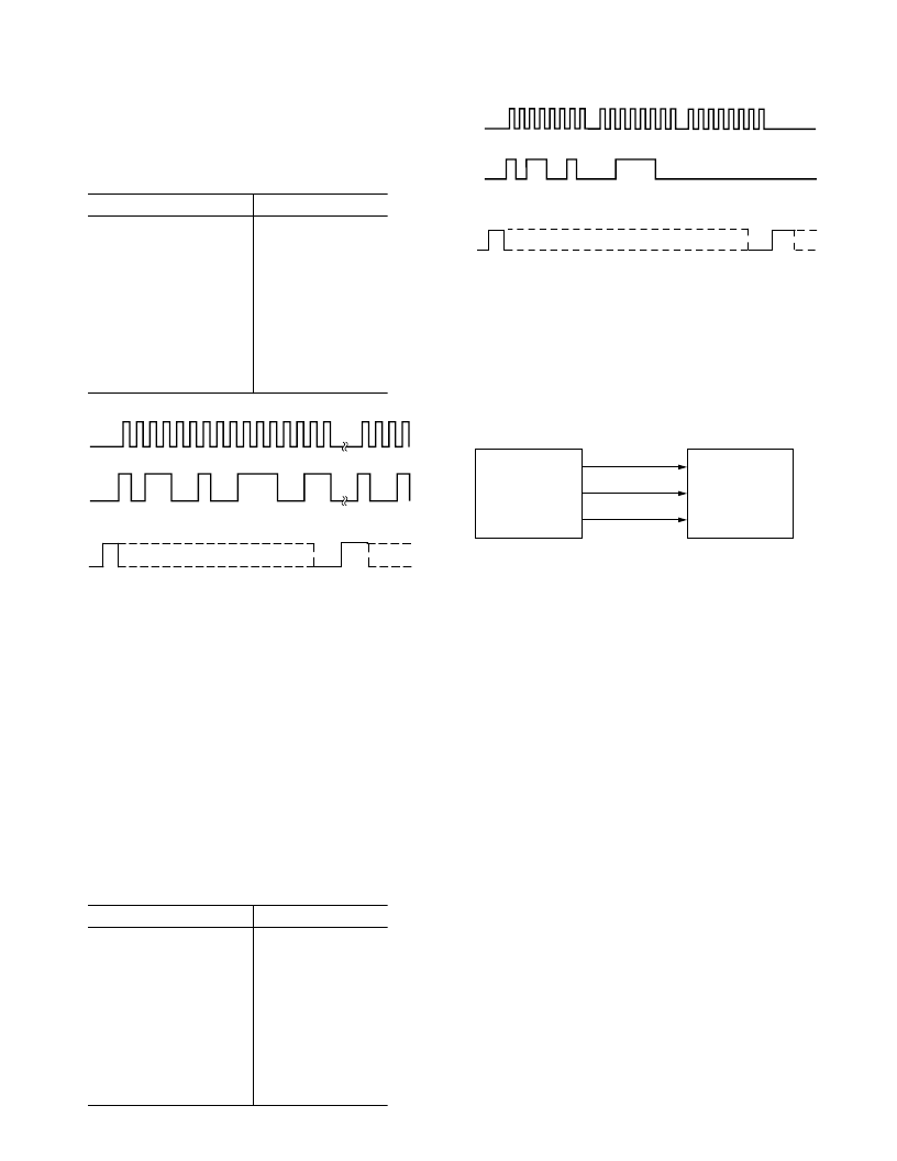
Figure 7. Write Cycle for Programming Alarm Current
Data
MICROPROCESSOR INTERFACING
AD421 – MC68HC11 (SPI BUS) INTERFACE
Figure 8 shows a typical interface between the AD421 and the
Motorola MC68HC11 SPI (Serial Peripheral Interface) bus.
The SCK, MOSI and SS pins of the 68HC11 are respectively
connected to the CLOCK, DATA IN and LATCH pins of the
AD421.
SCK
MOSI
SS
CLOCK
DATA IN
LATCH
AD421*
68HC11
* ADDITIONAL PINS OMITTED FOR CLARITY
Figure 8. AD421 to 68HC11 Interface
A typical routine such as the one shown below begins by initializ-
ing the state of the various SPI data and control registers.
INIT
LDAA #$2F
STAA
LDAA #$38
STAA
LDAA #$50
STAA
;
SS
= 1; SCK = 0; MOSI = 1
;SEND TO SPI OUTPUTS
;
SS
, SCK, MOSI = OUTPUTS
;SEND DATA DIRECTION INFO
;DABL INTRPTS, SPI IS MASTER & ON
;CPOL = 0, CPHA = 0, 1MHZ BAUDRATE
;LOAD ACCUM W/UPPER 8 BITS
SENDAT ;JUMP TO DAC OUTPUT ROUTINE
NEXTPT ;INFINITE LOOP
#$1000
;POINT AT ON-CHIP REGISTERS
$08,Y,$20 ;DRIVE
SS
(LATCH) LOW
SPDR
;SEND MS-BYTE TO SPI DATA REG
LDAA SPSR
;CHECK STATUS OF SPIE
BPL
WAIT1
;POLL FOR END OF X-MISSION
LDAA LSBY
;GET LOW 8 BITS FROM MEMORY
STAA
SPDR
;SEND LS-BYTE TO SPI DATA REG
LDAA SPSR
;CHECK STATUS OF SPIE
BPL
WAIT2;
;POLL FOR END OF X-MISSION
BSET
$08,Y,$20 ;DRIVE
SS
HIGH TO LATCH DATA
RTS
The SPI data port is configured to process data in 8-bit bytes.
The most significant data byte (MSBY) is retrieved from
memory and processed by the SENDAT routine. The
SS
pin is
driven low by indexing into the PORTD data register and clear
Bit 5. The MSBY is then sent to the SPI data register where it is
automatically transferred to the AD421 internal shift resistor.
PORTD
DDRD
SPCR
NEXTPT LDAA MSBY
BSR
JMP
SENDAT LDY
BCLR
STAA
WAIT1
WAIT2
of 11.147 mA. With 16 clock pulses between consecutive latch
signals data written is for normal 4 mA to 20 mA operation.
Table II. Ideal Input/Output Code Table
for 4 mA to 20 mA Operation
Code
Output Current
0000 0000 0000 0000
0000 0000 0000 0001
0000 0000 0000 0010
0100 0000 0000 0000
1000 0000 0000 0000
1100 0000 0000 0000
1111 1111 1111 1101
1111 1111 1111 1110
1111 1111 1111 1111
4 mA
4.000244 mA
4.000488 mA
8 mA
12 mA
16 mA
19.999268 mA
19.999512 mA
19.999756 mA
WORD "N"
WORD "N +1"
1
0
1 1
1
1
1
1 1
1
0
0
0
0
0 0
1
0 0
1
CLOCK
DATA
(
(
B
B
B
B
B
B
B
B
B
B
B
B
B
B
B
B
B
B
B
B
LATCH
Figure 6. Write Cycle for 4 mA to 20 mA Operation
Alarm Current Coding
Table III shows the ideal input-code-to-output-current relation-
ship for alarm current programming of the AD421. In this case,
the equivalent span is 0 mA to 32 mA but a reliable operating
span is 3.5 mA to 24 mA. The part may give an indeterminate
output for code values outside the range given in the table. As a
result, the user is advised to restrict the code programmed to the
part in alarm current mode to within the range shown in Table
III. Figure 7 shows a timing diagram for loading an alarm cur-
rent of 3.75 mA to the AD421 with an 8-bit microcontroller
using three 8-bit writes.
The output current values shown assume a REF IN voltage of
+2.5 V. With a REF IN of +2.5 V, an ideal 1 LSB = 32 mA/
131,072 = 244 nA.
Table III. Ideal Input/Output Code Table
for Alarm Current Operation
Code
Output Current
0 0011 1000 0000 0000
0 0011 1100 0000 0000
0 0100 0000 0000 0000
0 1000 0000 0000 0000
1 0000 0000 0000 0000
1 0100 0000 0000 0000
1 0110 0000 0000 0000
1 1000 0000 0000 0000
3.5 mA
3.75 mA
4 mA
8 mA
16 mA
20 mA
22 mA
24 mA
发布紧急采购,3分钟左右您将得到回复。
相关PDF资料
Eval-AD5025EBZ
Fully Accurate 12-/14-/16-Bit VOUT DAC SPI Interface 2.7 V to 5.5 V in a TSSOP
Eval-AD5045EBZ
Fully Accurate 12-/14-/16-Bit VOUT DAC SPI Interface 2.7 V to 5.5 V in a TSSOP
Eval-AD5065EBZ
Fully Accurate 12-/14-/16-Bit VOUT DAC SPI Interface 2.7 V to 5.5 V in a TSSOP
EVAL-AD5066EBZ
Fully Accurate 16-Bit UnBuffered VOUT DAC SPI Interface 2.7 V to 5.5 V in a TSSOP
EVAL-AD5379EB
40-Channel, 14-Bit, Parallel and Serial Input, Bipolar Voltage-Output DAC
EVAL-AD5381EB
40-Channel, 3 V/5 V, Single-Supply, 12-Bit, Voltage Output DAC
EVAL-AD5382EB
32-Channel, 3 V/5 V, Single-Supply, 14-Bit, Voltage Output DAC
EVAL-AD5383EB
32-Channel, 3 V/5 V, Single-Supply, 12-Bit, Voltage Output DAC
相关代理商/技术参数
EVAL-AD5025EBZ
制造商:AD 制造商全称:Analog Devices 功能描述:Fully Accurate 12-/14-/16-Bit VOUT DAC SPI Interface 2.7 V to 5.5 V in a TSSOP
EVAL-AD5045EBZ
制造商:AD 制造商全称:Analog Devices 功能描述:Fully Accurate 12-/14-/16-Bit VOUT DAC SPI Interface 2.7 V to 5.5 V in a TSSOP
EVAL-AD5060EB
制造商:Analog Devices 功能描述:EVAL BD FOR AD506X DAC 14-/16BIT, SERL INPUT - Bulk
EVAL-AD5060EBZ
功能描述:BOARD EVAL FOR AD5060 RoHS:是 类别:编程器,开发系统 >> 评估板 - 数模转换器 (DAC) 系列:nanoDAC™ 产品培训模块:Lead (SnPb) Finish for COTS
Obsolescence Mitigation Program 标准包装:1 系列:- DAC 的数量:4 位数:12 采样率(每秒):- 数据接口:串行,SPI? 设置时间:3µs DAC 型:电流/电压 工作温度:-40°C ~ 85°C 已供物品:板 已用 IC / 零件:MAX5581
EVAL-AD5061EBZ
功能描述:BOARD EVALUATION AD5061 RoHS:是 类别:编程器,开发系统 >> 评估板 - 数模转换器 (DAC) 系列:nanoDAC™ 产品培训模块:Lead (SnPb) Finish for COTS
Obsolescence Mitigation Program 标准包装:1 系列:- DAC 的数量:4 位数:12 采样率(每秒):- 数据接口:串行,SPI? 设置时间:3µs DAC 型:电流/电压 工作温度:-40°C ~ 85°C 已供物品:板 已用 IC / 零件:MAX5581
EVAL-AD5062EB
制造商:Analog Devices 功能描述:EVAL BD FOR AD506X DAC 14-/16BIT, SERL INPUT - Bulk
EVAL-AD5062EBZ
功能描述:BOARD EVAL FOR AD5062 RoHS:是 类别:编程器,开发系统 >> 评估板 - 数模转换器 (DAC) 系列:nanoDAC™ 产品培训模块:Lead (SnPb) Finish for COTS
Obsolescence Mitigation Program 标准包装:1 系列:- DAC 的数量:4 位数:12 采样率(每秒):- 数据接口:串行,SPI? 设置时间:3µs DAC 型:电流/电压 工作温度:-40°C ~ 85°C 已供物品:板 已用 IC / 零件:MAX5581
EVAL-AD5063EB
制造商:Analog Devices 功能描述:Evaluation Board For 14-/16-Bit, Serial Input, Vout NanoDACs 制造商:Analog Devices 功能描述:EVAL BD FOR AD506X DAC 14-/16BIT, SERL INPUT - Bulk